Menu

Blog

Archive for the ‘computing’ category: Page 518

Jan 6, 2021

Supercapacitors Challenge Batteries: Powerful Graphene Hybrid Material for Highly Efficient Energy Storage

Posted by in categories: chemistry, computing, mobile phones, sustainability, transportation

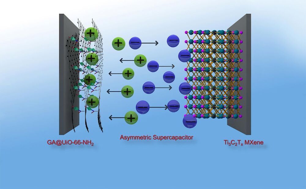
A team working with Roland Fischer, Professor of Inorganic and Metal-Organic Chemistry at the Technical University Munich (TUM) has developed a highly efficient supercapacitor. The basis of the energy storage device is a novel, powerful and also sustainable graphene hybrid material that has comparable performance data to currently utilized batteries.

Usually, energy storage is associated with batteries and accumulators that provide energy for electronic devices. However, in laptops, cameras, cellphones or vehicles, so-called supercapacitors are increasingly installed these days.

Unlike batteries they can quickly store large amounts of energy and put it out just as fast. If, for instance, a train brakes when entering the station, supercapacitors are storing the energy and provide it again when the train needs a lot of energy very quickly while starting up.

Jan 6, 2021

Convex to concave: More metasurface moiré results in wide-range lens

Posted by in categories: computing, drones, engineering, mobile phones, particle physics, virtual reality

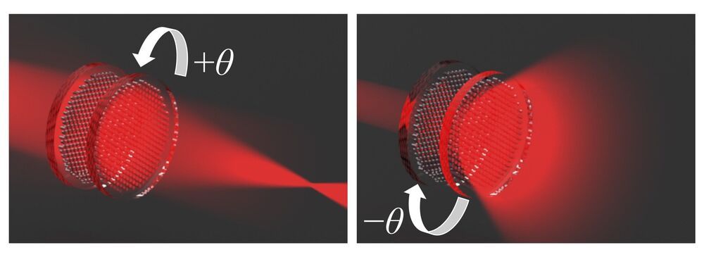
The odd, wavy pattern that results from viewing certain phone or computer screens through polarized glasses has led researchers to take a step toward thinner, lighter-weight lenses. Called moiré, the pattern is made by laying one material with opaque and translucent parts at an angle over another material of similar contrast.

A team of researchers from Tokyo University of Agriculture and Technology, TUAT, in Japan have demonstrated that moiré metalenses—tiny, patterned lenses composed of artificial ‘meta’ atoms—can tune along a wider range than previously seen. They published their results on November 23 in Optics Express.

“Metalenses have attracted a lot of interest because they are so thin and lightweight, and could be used in ultra-compact imaging systems, like future smart phones, virtual reality goggles, drones or microbots,” said paper author Kentaro Iwami, associate professor in the TUAT Department of Mechanical Systems Engineering.

Jan 5, 2021

Multifunctional lens sensor system could revolutionize smart contacts

Posted by in categories: biotech/medical, computing, health, internet, sustainability

The enormous impact of the recent COVID-19 pandemic, together with other diseases or chronic health risks, has significantly prompted the development and application of bioelectronics and medical devices for real-time monitoring and diagnosing health status. Among all these devices, smart contact lenses attract extensive interests due to their capability of directly monitoring physiological and ambient information. Smart contact lenses equipped with high sensitivity sensors would open the possibility of a non-invasive method to continuously detect biomarkers in tears. They could also be equipped with application-specific integrated circuit chips to further enrich their functionality to obtain, process and transmit physiological properties, manage illnesses and health risks, and finally promote health and wellbeing. Despite significant efforts, previous demonstrations still need multistep integration processes with limited detection sensitivity and mechanical biocompatibility.

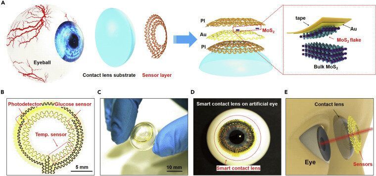
Recently, researchers from the University of Surrey, National Physical Laboratory (NPL), Harvard University, University of Science and Technology of China, Zhejiang University Ningbo Research Institute, etc. have developed a multifunctional ultrathin contact sensor system. The sensor systems contain a photodetector for receiving optical information, imaging and vision assistance, a temperature sensor for diagnosing potential corneal disease, and a glucose sensor for monitoring glucose level directly from the tear fluid.

Dr. Yunlong Zhao, Lecturer in Energy Storage and Bioelectronics at the Advanced Technology Institute (ATI), University of Surrey and Senior Research Scientist at the UK National Physical Laboratory (NPL), who led this research stated, “These results provide not only a novel and easy-to-make method for manufacturing advanced smart contact lenses but also a novel insight of designing other multifunctional electronics for Internet of Things, , etc.” Dr. Zhao added, “our ultrathin transistors-based serpentine mesh sensor system and fabrication strategy allow for further incorporation of other functional components, such as electrode array for electrophysiology, antennas for wireless communication, and the power modules, e.g. thin-film batteries and enzymatic biofuel cell for future in vivo exploration and practical application. Our research team at ATI, University of Surrey and NPL are currently working on these fields.”
Jan 5, 2021

New Quantum Algorithms Finally Crack Nonlinear Equations

Posted by in categories: computing, information science, quantum physics

Two teams found different ways for quantum computers to process nonlinear systems by first disguising them as linear ones.

Jan 4, 2021

Trapping light without back reflections

Posted by in categories: computing, drones

Researchers demonstrate a new technique for suppressing back reflections of light—better signal quality for sensing and information technology.

Microresonators are small glass structures in which light can circulate and build up in intensity. Due to material imperfections, some amount of light is reflected backwards, which is disturbing their function.

Continue reading “Trapping light without back reflections” »

Jan 4, 2021

Good News For Sailors: High Tech Lasers Could Replace Needle Guns

Posted by in categories: computing, transportation

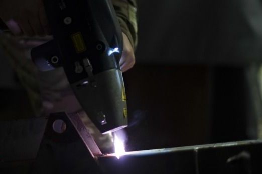
The U.S. Navy is testing out a new solution to the age-old problem of prepping for painting. Instead of chipping, sandblasting or hydroblasting, it is adopting technology from the aerospace sector: laser ablation.

Teams at Puget Sound Naval Shipyard are already using a laser paint stripping system that was originally developed by Missouri-based tech company Adapt Laser for use on aircraft components. The device peels off rust, paint, oil and other contaminants without leaving any residue or damaging the substrate. Instead of a dust of chips, rust and blasting grit on the surface, it leaves clean and ready-to-paint bare steel, according to the Navy.

7th Fleet’s shipyard at Yokosuka (Ship Repair Facility and Japan Regional Maintenance Center, or SRF-JRMC) is looking at bringing laser ablation into its yard in order to improve conditions for its workforce and accelerate its workflow. When considering prep time, the stripping process and post-stripping cleanup, laser ablation may be faster than some traditional surface preparation processes, according to Naval Sea Systems Command (NAVSEA).

Jan 3, 2021

Scientists Replicate Self-Cleaning Anti-reflective Nanocoating of Insects’ Eyes

Posted by in categories: biotech/medical, computing, economics, media & arts, nanotechnology

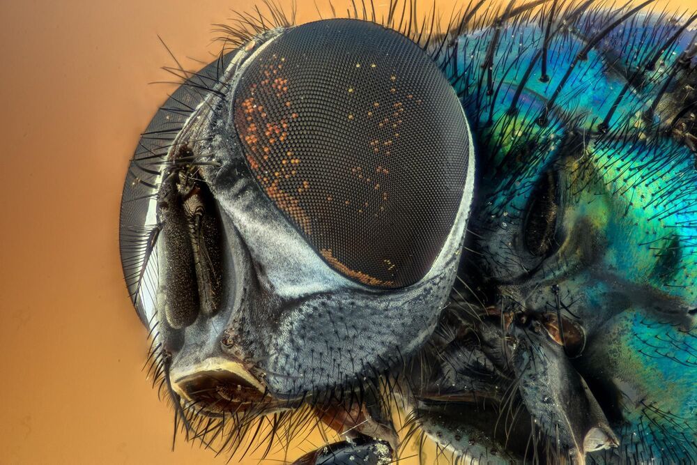
Scientists from Russia and Switzerland have probed into nanostructures covering the corneas of the eyes of small fruit flies. Investigating them the team learned how to produce the safe biodegradable nanocoating with antimicrobial, anti-reflective, and self-cleaning properties in a cost-effective and eco-friendly way. The protection coating might find applications in diverse areas of economics including medicine, nanoelectronics, automotive industry, and textile industry. The article describing these discoveries appears in Nature.

Scientists from Far Eastern Federal University (FEFU, Russia) teamed up with colleagues from University of Geneva, The University of Lausanne, and Swiss Federal Institute of Technology in Zurich for an interdisciplinary research project during which they were able to artificially reproduce the nanocoating of the corneas of fruit flies (Drosophila flies) naturally designed to protect the eyes of the insects from the smallest dust particles and shut off the reflection of light.

The craft of nanocoating meets demands in various fields of economics. It can wrap up any flat or three-dimensional structure, and, depending on the task, give it anti-reflective, antibacterial, and hydrophobic properties, including self-cleaning. The latter, for example, is a very important feature for expensive reusable overnight ortho-k lenses that correct the eyesight. Similar anti-reflective coatings are already known though created by more complex and costly methods. They are being used on the panels of computers, glasses, paintings in museums can be covered with them in order to exclude reflection and refraction of light.

Jan 2, 2021

Brains Behind the Brains: Mike Davies and Neuromorphic Computing at Intel Labs | Intel

Posted by in categories: computing, neuroscience

https://www.youtube.com/watch?v=GN3eSMoJcM8

Neuromorphic computing is coming, and it’s based on the way the brain works. In this installment of Brains Behind the Brains, Mike Davies, Director of Neuromorphic Computing at Intel Labs, talks to us about this technology, Intel’s Loihi processors, and how neuromorphic computing will change our world in wonderful ways. https://intel.ly/3hmL0Ip.

Subscribe now to Intel on YouTube: http://bit.ly/1BZDtpf.

Continue reading “Brains Behind the Brains: Mike Davies and Neuromorphic Computing at Intel Labs | Intel” »

Jan 2, 2021

Elastic diamonds could help quantum computers run at room temperature

Posted by in categories: computing, quantum physics

Scientists put diamonds under strain to improve their mechanical properties. The results suggest they may help quantum computers run at room temperature.

Jan 2, 2021

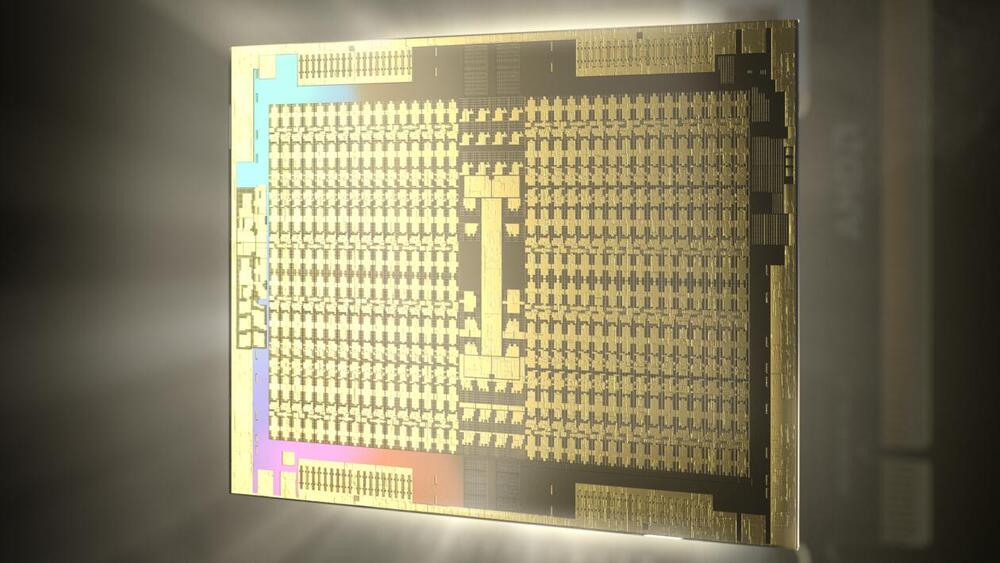
AMD Files MCM Based GPU Patent — Finally Bringing The MCM Approach To Radeon GPUs?

Posted by in categories: computing, futurism

AMD has filed a patent for something that everyone knew would eventually happen: an MCM GPU Chiplet design. Spotted by LaFriteDavid over at Twitter and published on Freepatents.com, the document shows how AMD plans to build a GPU chiplet graphics card that is eerily reminiscent of its MCM based CPU designs. With NVIDIA working on its own MCM design with Hopper architecture, it’s about time that we left monolithic GPU designs in the past and enable truly exponential performance growth.

AMD patents GPU chiplet design for future graphics cards

The patent points out that one of the reasons why MCM GPUs have not been attempted in the past is due to the high latency between chiplets, programming models and it being harder to implement parallelism. AMD’s patent attempts to solve all these problems by using an on-package interconnect it calls the high bandwidth passive crosslink. This would enable each GPU chiplet to communicate with the CPU directly as well as other chiplets via the passive crosslink. Each GPU would also feature its own cache. This design appears to suggest that each GPU chiplet will be a GPU in its own right and fully addressable by the operating system.