Researchers demonstrated microsecond-scale coherence times in a carbon nanotube quantum circuit, surpassing previous records.
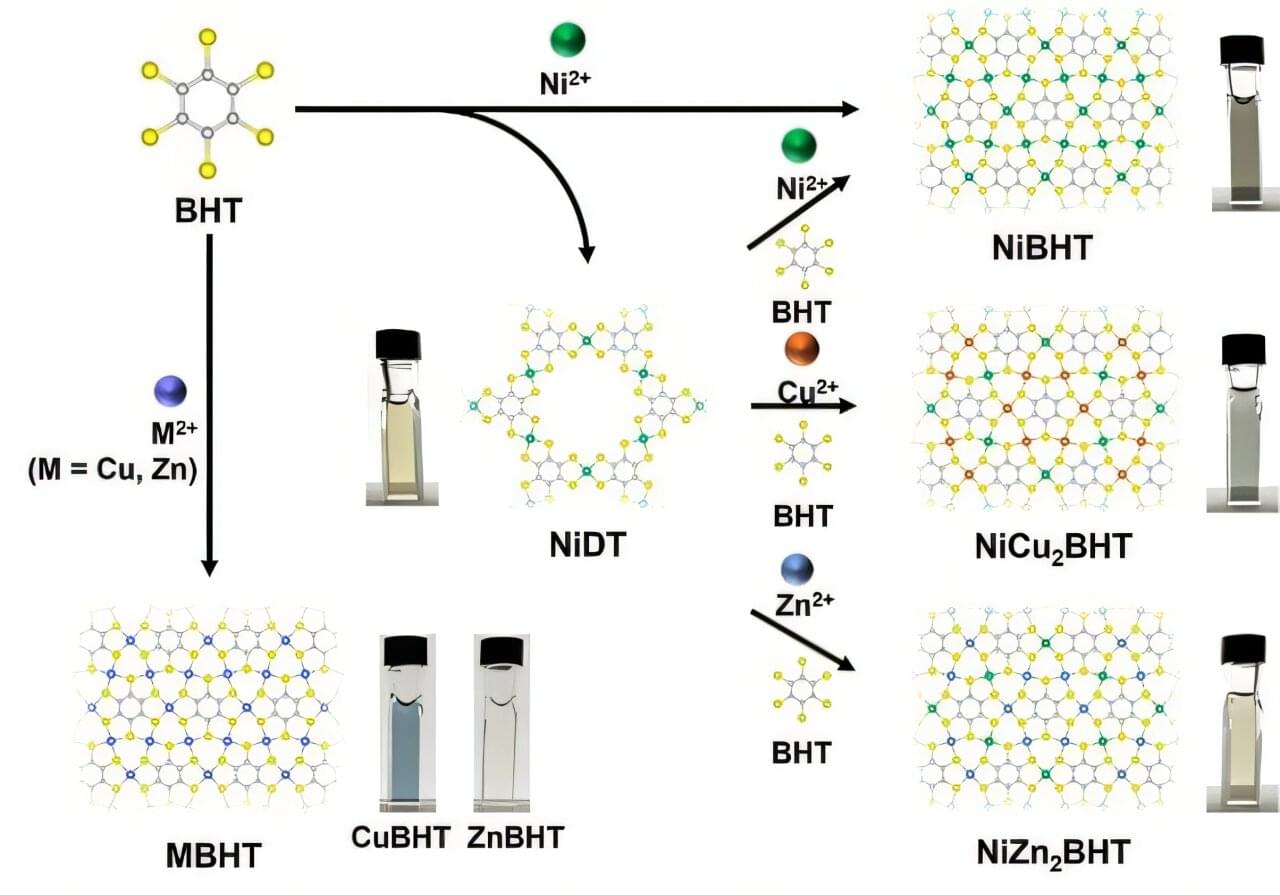
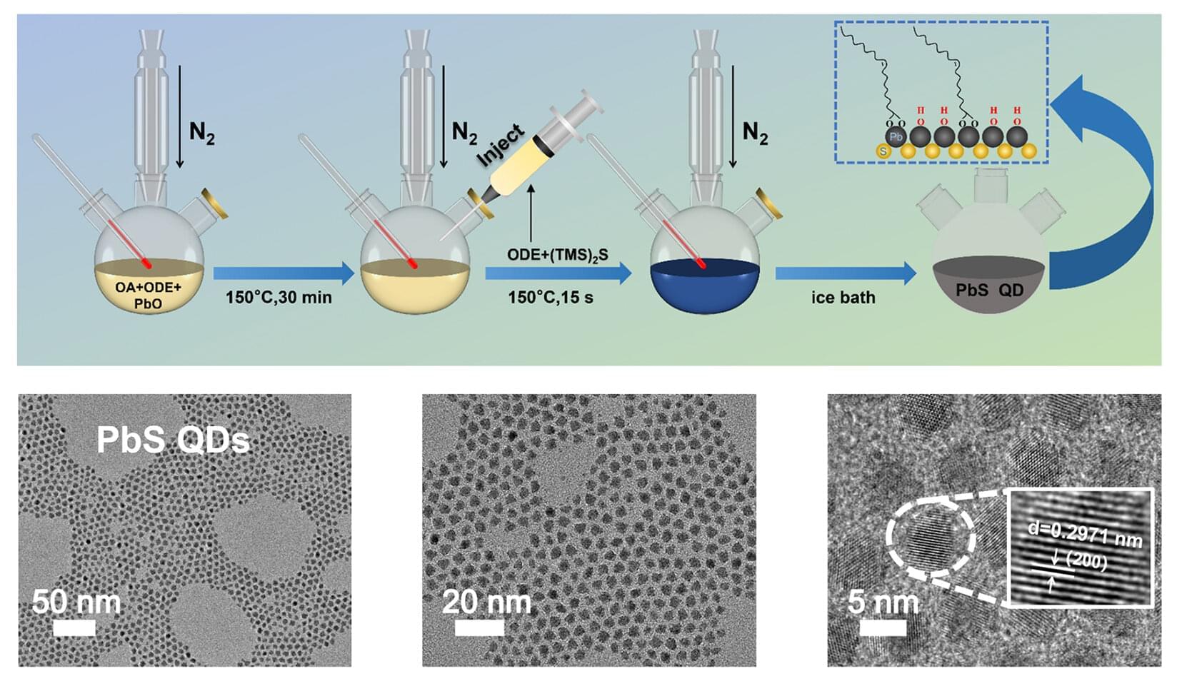
Coordination nanosheets are a unique class of two-dimensional (2D) materials that are formed by coordination bonds between planar organic ligands and metal ions. These 2D nanomaterials are increasingly utilized in energy storage, electronic devices, and as electrode-based catalysts due to their excellent electronic, optical, redox properties, and catalytic activity.
Over the last decade, coordination nanosheets composed of various transition metal ions, such as nickel (Ni) ions linked to benzenehexathiol (BHT)—an organic compound—have been successfully synthesized in laboratories. However, their production has relied on a two-phase interfacial reaction that occurs between two immiscible phases of matter.
Furthermore, the selective synthesis of well-organized heterometallic nanosheets, containing two or more metal ions, has proven to be difficult. To address these two major issues limiting the production of novel coordination nanosheets, a team of researchers led by Professor Hiroshi Nishihara, from the Research Institute for Science and Technology (RIST), Tokyo University of Science (TUS), Japan, has conducted a series of innovative experiments.
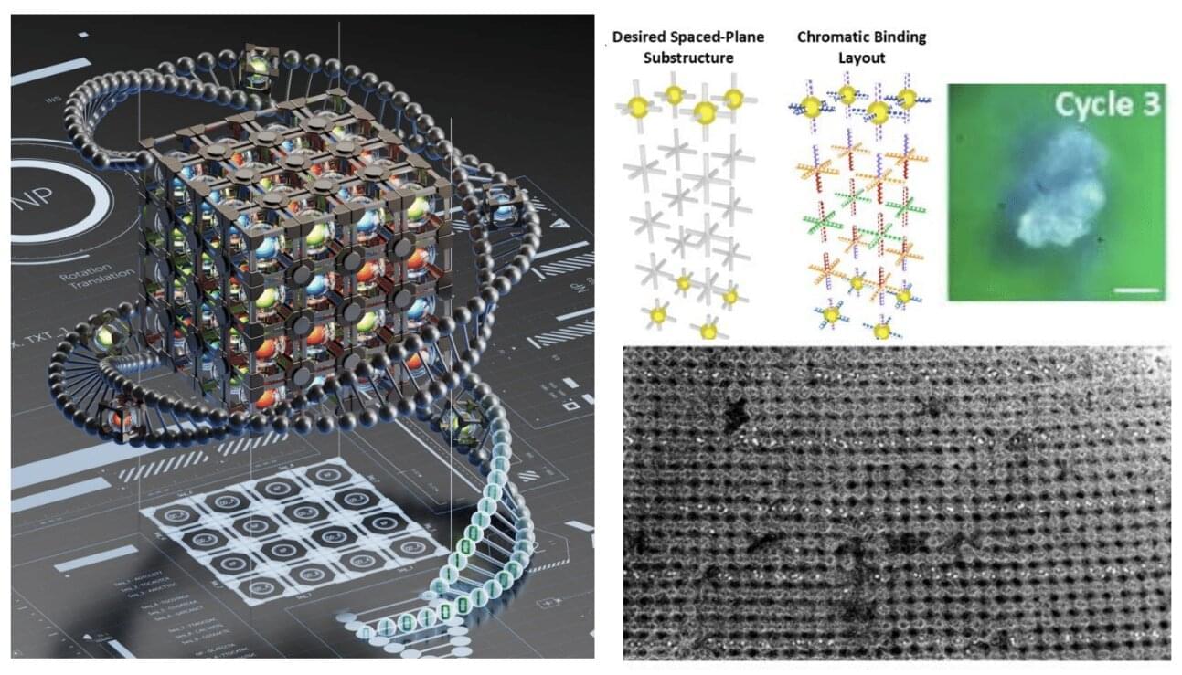
When the Empire State Building was constructed, its 102 stories rose above midtown one piece at a time, with each individual element combining to become, for 40 years, the world’s tallest building. Uptown at Columbia, Oleg Gang and his chemical engineering lab aren’t building Art Deco architecture; their landmarks are incredibly small devices built from nanoscopic building blocks that arrange themselves.
“We can now build the complexly prescribed 3D organizations from self-assembled nanocomponents, a kind of nanoscale version of the Empire State Building,” said Gang, professor of chemical engineering and of applied physics and materials science at Columbia Engineering and leader of the Center for Functional Nanomaterials’ Soft and Bio Nanomaterials Group at Brookhaven National Laboratory.
“The capabilities to manufacture 3D nanoscale materials by design are critical for many emerging applications, ranging from light manipulation to neuromorphic computing, and from catalytic materials to biomolecular scaffolds and reactors,” said Gang.
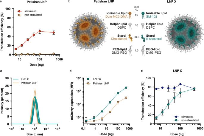
A major hurdle to curing HIV is the persistence of integrated proviruses in resting CD4+ T cells that remain in a transcriptionally silent, latent state. One strategy to eradicate latent HIV is to activate viral transcription, followed by elimination of infected cells through virus-mediated cytotoxicity or immune-mediated clearance. We hypothesised that mRNA-lipid nanoparticle (LNP) technology would provide an opportunity to deliver mRNA encoding proteins able to reverse HIV latency in resting CD4+ T cells. Here we develop an LNP formulation (LNP X) with unprecedented potency to deliver mRNA to hard-to-transfect resting CD4+ T cells in the absence of cellular toxicity or activation. Encapsulating an mRNA encoding the HIV Tat protein, an activator of HIV transcription, LNP X enhances HIV transcription in ex vivo CD4+ T cells from people living with HIV. LNP X further enables the delivery of clustered regularly interspaced short palindromic repeats (CRISPR) activation machinery to modulate both viral and host gene transcription. These findings offer potential for the development of a range of nucleic acid-based T cell therapeutics.
Resting T cells are difficult to manipulate, and are a reservoir for latent HIV. Here, the authors develop a lipid nanoparticle formulation with the ability to transfect resting primary human T cells, enabling delivery of mRNAs that result in reactivation of latent HIV. This could help development of HIV cure strategies.
Imagine a high-tech workshop where scientists and engineers craft objects so small they can’t be seen with the naked eye — or even a standard microscope. These tiny structures — nanostructures — are thousands of times smaller than a strand of hair. And they are essential for faster computers, better smartphones and life-saving medical devices.
Nanostructures are at the core of the research happening every day in the Washington Nanofabrication Facility (WNF). Part of the Institute for Nano-Engineered Systems at the UW and located in Fluke Hall, the WNF supports cutting-edge academic and industry research, prototyping and hands-on student training. Like many leading nanofabrication centers, it is part of the National Science Foundation’s National Nanotechnology Coordinated Infrastructure, a network that shares expertise and resources.
Step inside the Washington Nanofabrication Facility, where tiny tech is transforming research in quantum, chips, medicine and more.
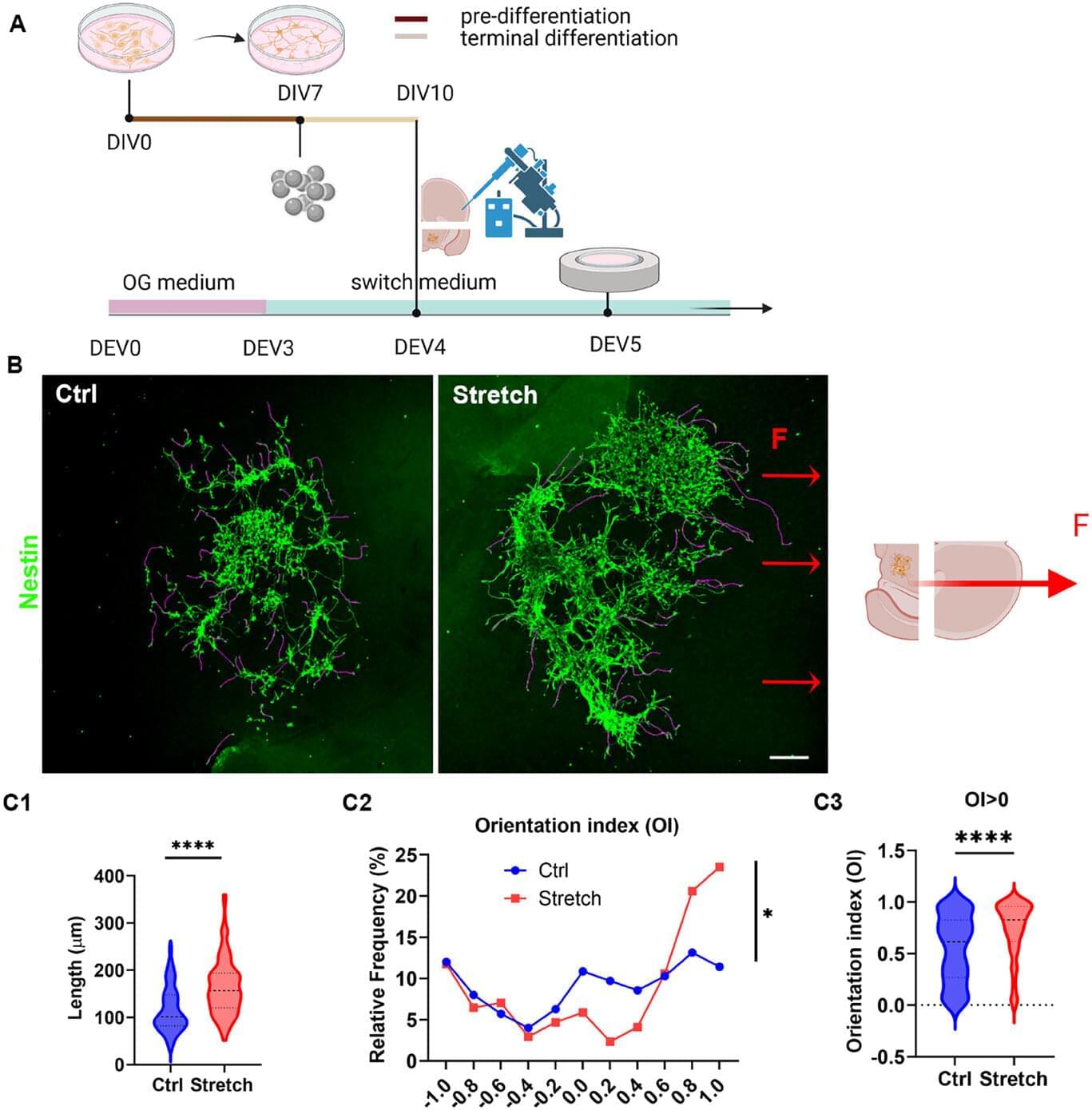
A collaborative study led by Professor Vittoria Raffa at the University of Pisa and Assistant Professor Fabian Raudzus (Department of Clinical Application) has unveiled a novel approach that uses magnetically guided mechanical forces to direct axonal growth, aiming to enhance the effectiveness of stem cell-based therapies for Parkinson’s disease (PD) and other neurological conditions.
Parkinson’s disease is characterized by the progressive degeneration of dopaminergic neurons in the substantia nigra (SN), which project to the striatum (ST) via the nigrostriatal pathway. The loss of these connections leads to dopamine deficiency and the onset of motor symptoms.
While cell replacement therapies using human stem cell-derived dopaminergic progenitors have shown encouraging results in clinical trials, a key limitation remains: the inability to guide the axons of transplanted cells over long distances to their appropriate targets in the adult brain.
A USA company is producing nano-sulfide solid-electrolyte powders for use in batteries.
To try everything Brilliant has to offer—free—for a full 30 days, visit https://brilliant.org/ArtemKirsanov. You’ll also get 20% off an annual premium subscription.
Socials:
X/Twitter: https://twitter.com/ArtemKRSV
Patreon: https://patreon.com/artemkirsanov.
My name is Artem, I’m a graduate student at NYU Center for Neural Science and researcher at Flatiron Institute. In this video we explore a recent study published in Science, which revealed that different compartments of pyramidal neurons (apical vs basal dendrites) use different plasticity rules for learning.
Link to the paper:
https://www.science.org/doi/10.1126/science.ads4706
Outline:
00:00 Introduction.
01:23 Synaptic transmission.
06:09 Molecular machinery of LTP
08:40 Hebbian plasticity.
11:21 Non-Hebbian plasticity.
12:51 Hypothesis.
14:42 Experimental methods.
17:10 Result: compartmentalized plasticity.
19:30 Interpretation.
22:01 Brilliant.
23:08 Outro.
Music by Artlist.

In blinding bright light or pitch-black dark, our eyes can adjust to extreme lighting conditions within a few minutes. The human vision system, including the eyes, neurons, and brain, can also learn and memorize settings to adapt faster the next time we encounter similar lighting challenges.
In an article published in Applied Physics Letters, researchers at Fuzhou University in China created a machine vision sensor that uses quantum dots to adapt to extreme changes in light far faster than the human eye can—in about 40 seconds—by mimicking eyes’ key behaviors. Their results could be a game changer for robotic vision and autonomous vehicle safety.
“Quantum dots are nano-sized semiconductors that efficiently convert light to electrical signals,” said author Yun Ye.