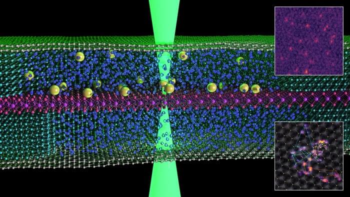
A new technique makes it possible to capture videos of single atoms “swimming” at the interface between a solid and a liquid for the first time. The approach uses stacks of two-dimensional materials to trap the liquid, making it compatible with characterization techniques that usually require vacuum conditions. It could enable researchers to better understand how atoms behave at these interfaces, which play a crucial role in devices such as batteries, catalytic systems and separation membranes.
Several techniques exist to image single atoms, including scanning tunnelling microscopy (STM) and transmission electron microscopy (TEM). However, they involve exposing atoms on the surface of the sample to a high-vacuum environment, which can change the material’s structure. Techniques that do not require a vacuum, meanwhile, are either lower-resolution or only work for short time periods, meaning that the atoms’ motion cannot be captured on video.
Researchers led by materials scientists Sarah Haigh of the University of Manchester’s National Graphene Institute (NGI) have now developed a new approach that enables them to track the motion of single atoms on a surface when that surface is surrounded by liquid. They showed that the atoms behave very differently under these circumstances than they do in vacuum. “This is crucial,” explains Haigh, “since we want to understand atomic behaviour for realistic reaction/environmental conditions that the material will experience in use – for example, in a battery, supercapacitor and membrane reaction vessels.”
