Toggle light / dark theme

Topological Materials Are Everywhere — New Database Reveals Over 90,000

Searchable tool reveals more than 90,000 known materials with electronic properties that remain unperturbed in the face of disruption.

What will it take for our electronics to become smarter, faster, and more resilient? One idea is to build them out of topological materials.

Topology stems from a branch of mathematics that studies shapes that can be manipulated or deformed without losing certain essential properties. A donut is a common example: If it were made of rubber, a donut could be twisted and squeezed into a completely new shape, such as a coffee mug, while retaining a key trait — namely, its center hole, which takes the form of the cup’s handle. The hole, in this case, is a topological trait, robust against certain deformations.

Paper-based semiconductor aids the drive for sustainable electronics

According to the team, the new semiconducting cellulose nanopaper (CNP) can be tailored for a variety of applications. The paper itself can be shaped into different designs and the material’s electrical conduction properties can be tuned from 1012 to 10–2 Ω cm – values that exceed those of previously-reported 3D semiconducting materials – by changing the concentration of charge carriers (electrons and holes) in it. This means it is suitable for use in many devices, from water vapour sensors to electrodes in enzymatic biofuel cells.

New electronics cooling tech enables 740% increase in power per unit volume

Tarek Gebrael, a UIUC Ph.D. student in mechanical engineering, explains that the existing solutions suffer from three shortcomings – first, they can be expensive and difficult to scale up. Second, conventional heat spreading approaches generally require that the heat spreader and a heat sink be attached on top of the electronics device. Unfortunately, in many cases, most of the heat is generated underneath the electronic devices, meaning that the cooling mechanism isn’t where it is needed the most.

And third, Gebrael explained, the heat spreaders can’t be installed directly on the surface of the electronics. They require a layer of “thermal interface material” sandwiched between them to ensure good contact. However, due to its poor heat transfer characteristics, that middle layer also introduces a negative impact on thermal performance.

Now, researchers have come up with a new solution to address all three of those problems. First, they used copper as a primary material, which is relatively inexpensive. They then made the copper coating that entirely “engulfs” the device, says Gebrael, “covering the top, the bottom, and the sides… a conformal coating that covers all the exposed surfaces” – so that no heat-producing regions are neglected. And finally, the new solution removes the need for a thermal interface material and a heat sink.

Imec Presents Sub-1nm Process and Transistor Roadmap Until 2036: From Nanometers to the Angstrom Era

Imec plots a course to 1nm chips, and beyond.


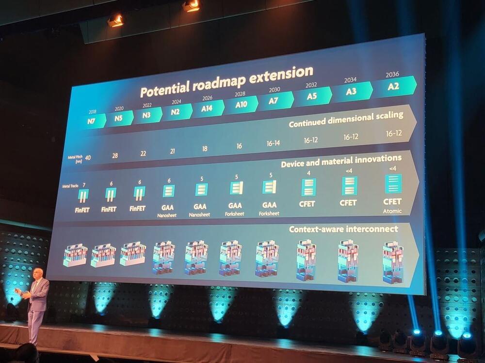
Imec, the most advanced semiconductor research firm in the world, recently shared its sub-‘1nm’ silicon and transistor roadmap at its Future Summit event in Antwerp, Belgium. The roadmap gives us a rough idea of the timelines through 2036 for the next major process nodes and transistor architectures the company will research and develop in its labs in cooperation with industry giants, like TSMC, Intel, Samsung, and ASML, among many others.

The roadmap includes breakthrough transistor designs that evolve from the standard FinFET transistors that will last until 3nm, to new Gate All Around (GAA) nanosheets and forksheet designs at 2nm and A7 (seven angstroms), respectively, followed by breakthrough designs like CFETs and atomic channels at A5 and A2. As a reminder, ten Angstroms are equal to 1nm, so Imec’s roadmap encompasses sub-‘1nm’ process nodes.

You might not have heard of the Interuniversity Microelectronics Centre (imec) before, but it ranks among the most important companies in the world, alongside better-known companies like TSMC and EUV-toolmaker ASML. Think of imec as a silicon Switzerland, of sorts. While the semiconductor research-focused imec doesn’t operate with much fanfare, it serves as the quiet cornerstone of the semiconductor industry, bringing fierce rivals like Intel, TSMC, and Samsung together with chip toolmakers such as ASML and Applied Materials, not to mention the equally-critical semiconductor software design companies (EDA) like Cadence and Synopsys, in a non-competitive environment. This collaboration allows the companies to work together to define the next generation of tools and software they will use to design and manufacture the chips that power the world.

Spin keeps electrons in line in iron-based superconductor

Researchers from PSI’s Spectroscopy of Quantum Materials group together with scientists from Beijing Normal University have solved a puzzle at the forefront of research into iron-based superconductors: the origin of FeSe’s electronic nematicity. Using Resonant inelastic X-ray scattering (RIXS) at the Swiss Light Source (SLS), they discovered that, surprisingly, this electronic phenomenon is primarily spin driven.

Electronic nematicity is believed to be an important ingredient in high-temperature superconductivity, but whether it helps or hinders it is still unknown.

Their findings are published in Nature Physics (“Spin-excitation anisotropy in the nematic state of detwinned FeSe”).

The crucial role of functional motifs—microstructural units that govern material functions—in material research

The traditional trial-and-error method in material research cannot meet the growing demand of various high performance materials, so developing a new effective paradigm of material science is extremely urgent. A study led by Dr. Xiao-Ming Jiang and Prof. Guo-Cong Guo (Fujian Institute of Research on the Structure of Matter, Chinese Academy of Sciences) proposes a new research paradigm for material studies based on the “functional motif” concept.

Functional motif was defined as the critical microstructure units (e.g., constituent components and ) that play a decisive role in generating certain material functions. These units could not be replaced with other structure units without losing or significantly suppressing the relevant functions. The functional motif paradigm starts with the main aspects of microscopic structures and the properties of materials. On the basis of this understanding, the functional motifs governing the can be extracted and the quantitative relationships between them can be investigated, and the results could be further developed as the “functional motif theory.” The latter should be useful as a guideline for creating new materials and as a tool for predicting the physicochemical properties of materials.

The properties of materials are determined by their functional motifs and how they are arranged in the materials, with the latter determining the quantitative structure–property relationships. Uncovering the functional motifs and their arrangements is crucial in understanding the properties of materials, and the functional motif exploration enables the rational design of new materials with desired properties.

Physicists Say There May Be Another Reality Right Beyond This One

For those of us worried the world somehow got trapped in the wrong timeline, relax — scientists are now saying there might actually be two realities.

Two researchers from the University of Maryland released their findings in a study earlier this month in the journal Physical Review Research. According to a university press release, though, a second reality isn’t exactly what they set out to find. While studying layers of graphene, made with hexagons of carbon, the found repeating patterns that changed the way electricity moves.

Based on their research, the pair think they accidentally found a clue that could explain some of our current reality’s mysteries. According to the university’s media arm, they realized that experiments on the electrical properties of stacked sheets of graphene produced results that looked like little universes and that the underlying causes could apply to other areas of physics. In stacks of graphene, electricity changes behavior when two sheets interact, so the two hypothesize that unique physics could similarly emerge from interacting layers elsewhere—perhaps across the entire universe.

Fastest logic gates ever made could make computers 1,000,000x faster

Researchers have developed a new kind of logic gate, the fundamental building block from which computers are made. Depending on the kind of logic gate and its rules, two inputs of any combination of 0 and 1 result in an output of either a 1 or 0. A single chip used in creating electronic components like processors and memory modules can contain billions of logic gates.

The newly developed logic gate, which demonstrates the viability of “lightwave electronics,” works orders of magnitudes faster than traditional logic gates. Ordinary logic gates have an input processing delay on the order of nanoseconds, but the new logic gates process inputs in only femtoseconds, a million times shorter than nanoseconds.

The new gates comprise two gold electrodes connected with a graphene wire, which is then zapped with laser pulses, adjusting the pulse’s phase to produce outputs of either a one or a 0. The shortened processing time for the new logic gates means that computers built on the technology would have their processing speeds measured on Petahertz (PHz) scale compared to the current Gigahertz (GHz).