I may have already posted about this, but this is more data from The Lancet.
Background.
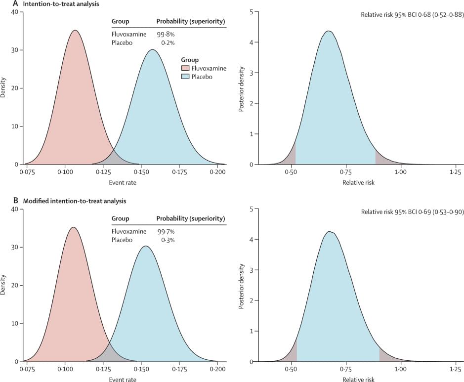
Recent evidence indicates a potential therapeutic role of fluvoxamine for COVID-19. In the TOGETHER trial for acutely symptomatic patients with COVID-19, we aimed to assess the efficacy of fluvoxamine versus placebo in preventing hospitalisation defined as either retention in a COVID-19 emergency setting or transfer to a tertiary hospital due to COVID-19.
Methods.
This placebo-controlled, randomised, adaptive platform trial done among high-risk symptomatic Brazilian adults confirmed positive for SARS-CoV-2 included eligible patients from 11 clinical sites in Brazil with a known risk factor for progression to severe disease. Patients were randomly assigned (1:1) to either fluvoxamine (100 mg twice daily for 10 days) or placebo (or other treatment groups not reported here). The trial team, site staff, and patients were masked to treatment allocation. Our primary outcome was a composite endpoint of hospitalisation defined as either retention in a COVID-19 emergency setting or transfer to tertiary hospital due to COVID-19 up to 28 days post-random assignment on the basis of intention to treat. Modified intention to treat explored patients receiving at least 24 h of treatment before a primary outcome event and per-protocol analysis explored patients with a high level adherence (80%). We used a Bayesian analytic framework to establish the effects along with probability of success of intervention compared with placebo. The trial is registered at ClinicalTrials dot gov (NCT04727424) and is ongoing.
Treatment with fluvoxamine (100 mg twice daily for 10 days) among high-risk outpatients with early diagnosed COVID-19 reduced the need for hospitalisation defined as retention in a COVID-19 emergency setting or transfer to a tertiary hospital.