Archive for the ‘materials’ category: Page 50
Mar 28, 2024
3D printed shapeshifting nanoparticles
Posted by Dan Breeden in categories: materials, nanotechnology
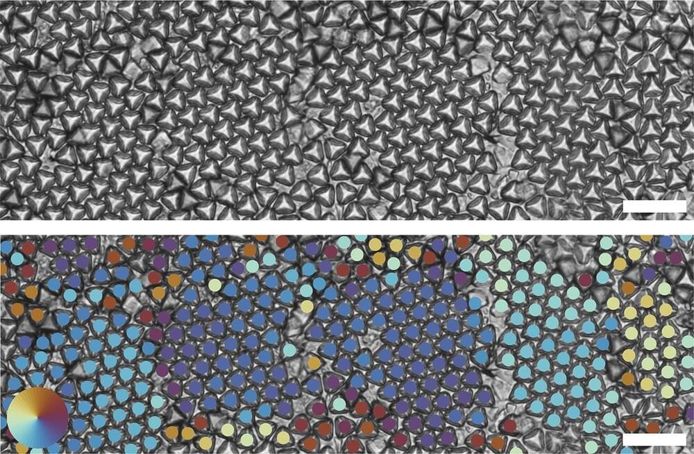
Stanford materials engineers have 3D printed tens of thousands of hard-to-manufacture nanoparticles long predicted to yield promising new materials that change form in an instant.
Mar 28, 2024
Bosonic Kitaev chain metamaterial to amplify sound waves, a first
Posted by Shubham Ghosh Roy in category: materials
New metamaterial revolutionizes sound wave amplification discovery:
Researchers have realized a new type of metamaterial through which sound waves flow in an unprecedented fashion.
Mar 28, 2024
Elusive 3D Printed Nanoparticles Could Lead to New Shapeshifting Materials
Posted by Shailesh Prasad in categories: materials, nanotechnology
Stanford materials engineers have 3D printed tens of thousands of hard-to-manufacture nanoparticles long predicted to yield promising new materials that change form in an instant.
Mar 27, 2024
New topological metamaterial amplifies sound waves exponentially
Posted by Dan Breeden in categories: electronics, materials
Researchers at AMOLF, in collaboration with partners from Germany, Switzerland, and Austria, have realized a new type of metamaterial through which sound waves flow in an unprecedented fashion. It provides a novel form of amplification of mechanical vibrations, which has the potential to improve sensor technology and information processing devices.
Mar 25, 2024
Weird new electron behaviour in stacked graphene thrills physicists
Posted by Cecile G. Tamura in categories: materials, quantum physics
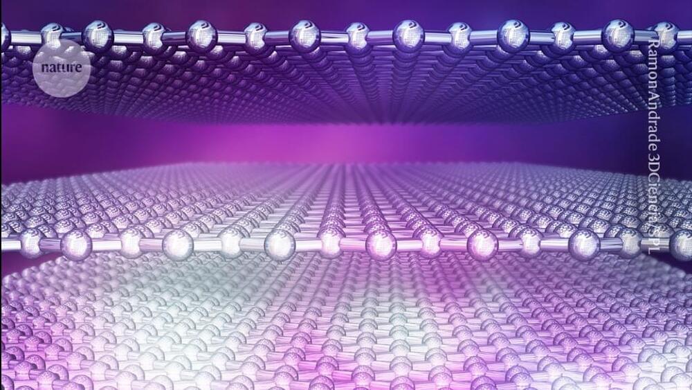
This 2D material is only the second to exhibit the fractional quantum anomalous Hall effect, and theorists are still debating how it works.
Mar 25, 2024
Exploring Extraterrestrial Oceans: Ice-Grains as Potential Carriers of Life
Posted by Laurence Tognetti, Labroots Inc. in categories: materials, space
“For the first time we have shown that even a tiny fraction of cellular material could be identified by a mass spectrometer onboard a spacecraft,” said Dr. Fabian Klenner.
How will we find life on Jupiter’s icy moon, Europa, and Saturn’s icy moon, Enceladus? This is what a recent study published in Science Advances hopes to address as a team of international researchers investigate how ice grains that are discharged from the active plumes of these small moons could possess enough organic material for life to exist. This study holds the potential to help astrobiologists develop the necessary instruments and methods to find life on these small moons, specifically with NASA’s Europa Clipper scheduled to launch this October, whose goal will be to investigate Europa’s habitability potential.
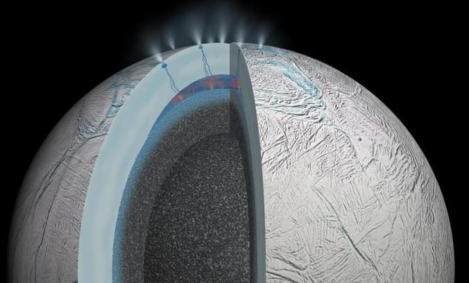
Artist’s illustration of Saturn’s moon, Enceladus, seen here upside down as the plumes are on the south pole. (Credit: NASA/JPL-Caltech)
Continue reading “Exploring Extraterrestrial Oceans: Ice-Grains as Potential Carriers of Life” »
Mar 22, 2024
Discovery of a hidden quantum critical point in two-dimensional superconductors
Posted by Dan Breeden in categories: materials, quantum physics
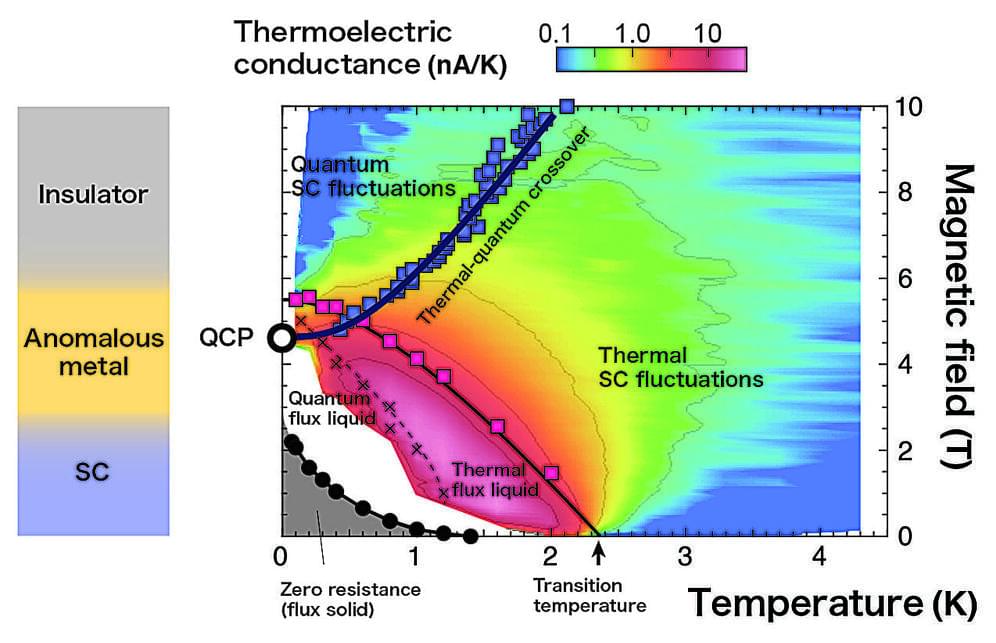
Weak fluctuations in superconductivity, a precursor phenomenon to superconductivity, have been successfully detected by a research group at the Tokyo Institute of Technology (Tokyo Tech). This breakthrough was achieved by measuring the thermoelectric effect in superconductors over a wide range of magnetic fields and over a wide range of temperatures, from much higher than the superconducting transition temperature to very low temperatures near absolute zero. The results of this study were published online in Nature Communications on March 16, 2024.
This revealed the full picture of fluctuations in superconductivity with respect to temperature and magnetic field, and demonstrated that the origin of the anomalous metallic state in magnetic fields—which has been an unsolved problem in the field of two-dimensional superconductivity for 30 years—is the existence of a quantum critical point, where quantum fluctuations are at their strongest.
Mar 22, 2024
These ‘Strange Metals’ Bend the Rules of Physics
Posted by Shubham Ghosh Roy in categories: materials, quantum physics
Electrons swarm in a soup of quantum entanglement in a new class of materials called strange metals.
Mar 22, 2024
Another Twist in the Understanding of Moiré Materials
Posted by Saúl Morales Rodriguéz in categories: materials, quantum physics
The unexpected observation of an aligned spin polarization in certain twisted semiconductor bilayers calls for improved models of these systems.
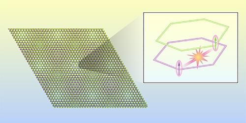
If you take two overlapping tiled patterns and rotate one with respect to the other, new patterns will emerge. This motif has been used in art and architecture for millennia. Over the past 15 years, materials physicists have used a similar strategy to realize new material properties. In one implementation, two material monolayers with a hexagonal atomic lattice are overlaid with an angle between the two lattices, resulting in an additional long-range lattice structure known as a moiré pattern. In 2021, scientists observed the so-called quantum anomalous Hall (QAH) effect in such a twisted bilayer, formed of MoTe2 and WSe2 monolayers [1]. Now Zui Tao at Cornell University and colleagues have used optical spectroscopy to study the interaction between these two monolayers when they are in the QAH state [2].

