Archive for the ‘quantum physics’ category: Page 399
Jun 28, 2022
Our universe was made by aliens in a lab, theorises Harvard scientist
Posted by Kelvin Dafiaghor in categories: biological, climatology, genetics, habitats, quantum physics, sustainability
Ever considered the notion that everything around you was cooked up by aliens in a lab? Theoretical physicist and former chair of Harvard’s astronomy department, Abraham ‘Avi’ Loeb, has proposed a wild – if unsettling – theory that our universe was intentionally created by a more advanced class of lifeform.
In an op-ed for Scientific American, “Was Our Universe Created In A Laboratory?”, Loeb suggested that aliens could have created a ‘baby universe’ using ‘quantum tunneling’, which would explain our universe’s ‘flat geometry’ with zero net energy. If this discovery were proven true, then the universe humans live in would be shown to be “like a biological system that maintains the longevity of its genetic material through multiple generations,” Loeb wrote.
Loeb put forward the idea of a scale of developed civilisations (A, B, etc.) and, due to that fact that on Earth we currently don’t have the ability to reproduce the astrophysical conditions that led to our existence, “we are a low-level technological civilisation, graded class C on the cosmic scale” (essentially: dumb). We would be higher up, he added, if we possessed the ability to recreate the habitable conditions on our planet for when the sun will die. But, due to our tendency to “carelessly destroy the natural habitat” on Earth through climate change, we should really be downgraded to class D.
Jun 28, 2022
Hysteresis and Stochastic Fluorescence
Posted by Shubham Ghosh Roy in categories: materials, quantum physics
“Blinking” behavior of fluorophores, being harmful for the majority of super-resolved techniques, turns into a key property for stochastic optical fluctuation imaging and its modifications, allowing one to look at the fluorophores already used in conventional microscopy, such as graphene quantum dots, from a completely new perspective. Here we discuss fluorescence of aggregated ensembles of graphene quantum dots structured at submicron scale. We study temperature dependence and stochastic character of emission. We show that considered quantum dots ensembles demonstrate rather complicated temperature-dependent intermittent emission, that is, “blinking” with a tendency to shorten “blinking” times with the increase of temperature.
Jun 28, 2022
Xanadu puts quantum advantage in the cloud
Posted by Dan Breeden in categories: particle physics, quantum physics
Toronto-based start-up’s programmable photonic device is accessible to the public and much faster than classical machines at Gaussian boson sampling.
Jun 28, 2022
Making dark semiconductors shine
Posted by Shubham Ghosh Roy in categories: computing, particle physics, quantum physics, solar power, sustainability
Whether or not a solid can emit light, for instance as a light-emitting diode (LED), depends on the energy levels of the electrons in its crystalline lattice. An international team of researchers led by University of Oldenburg physicists Dr. Hangyong Shan and Prof. Dr. Christian Schneider has succeeded in manipulating the energy-levels in an ultra-thin sample of the semiconductor tungsten diselenide in such a way that this material, which normally has a low luminescence yield, began to glow. The team has now published an article on its research in the science journal Nature Communications.
According to the researchers, their findings constitute a first step towards controlling the properties of matter through light fields. “The idea has been discussed for years, but had not yet been convincingly implemented,” said Schneider. The light effect could be used to optimize the optical properties of semiconductors and thus contribute to the development of innovative LEDs, solar cells, optical components and other applications. In particular the optical properties of organic semiconductors—plastics with semiconducting properties that are used in flexible displays and solar cells or as sensors in textiles—could be enhanced in this way.
Tungsten diselenide belongs to an unusual class of semiconductors consisting of a transition metal and one of the three elements sulfur, selenium or tellurium. For their experiments the researchers used a sample that consisted of a single crystalline layer of tungsten and selenium atoms with a sandwich-like structure. In physics, such materials, which are only a few atoms thick, are also known as two-dimensional (2D) materials. They often have unusual properties because the charge carriers they contain behave in a completely different manner to those in thicker solids and are sometimes referred to as “quantum materials.”
Jun 28, 2022
Taking quantum control of life’s building blocks
Posted by Dan Breeden in categories: alien life, chemistry, quantum physics
Life (as we know it) is based on carbon. Despite its ubiquity, this important element still holds plenty of secrets, on earth and in the heavens above us. For example, astrophysicists like Columbia’s Daniel Wolf Savin who study interstellar clouds want to understand how the chemicals, including carbon, swirling within these nebulous aggregations of gas and dust form the stars and planets that dot our universe and give rise to organic life.
Jun 28, 2022
Quantum Circuit Uses Just A Few Atoms
Posted by Dan Breeden in categories: computing, particle physics, quantum physics
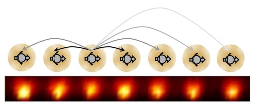
Researchers at the University of New South Wales and a startup company, Silicon Quantum Computing, published results of their quantum dot experiments. The circuits use up to 10 carbon-based quantum dots on a silicon substrate. Metal gates control the flow of electrons. The paper appears in Nature and you can download the full paper from there.
What’s new about this is that the dots are precisely arranged to simulate an organic compound, polyacetylene. This allowed researchers to model the actual molecule. Simulating molecules is important in the study of exotic matter phases, such as superconductivity. The interaction of particles inside, for example, a crystalline structure is difficult to simulate using conventional methods. By building a model using quantum techniques on the same scale and with the same topology as the molecule in question, simulation is simplified.
The SSH (Su-Schreffer-Heeger) model describes a single electron moving along a one-dimensional lattice with staggered tunnel couplings. At least, that’s what the paper says and we have to believe it. Creating such a model for simple systems has been feasible, but for a “many body” problem, conventional computing just isn’t up to the task. Currently, the 10 dot model is right at the limit of what a conventional computer can simulate reasonably. The team plans to build a 20 dot circuit that would allow for unique simulations not feasible with classic computing tech.
Jun 28, 2022
2D interfaces in future transistors may not be as flat as previously thought
Posted by Dan Breeden in categories: computing, mobile phones, particle physics, quantum physics
Transistors are the building blocks of modern electronics, used in everything from televisions to laptops. As transistors have gotten smaller and more compact, so have electronics, which is why your cell phone is a super powerful computer that fits in the palm of your hand.
But there’s a scaling problem: Transistors are now so small that they are difficult to turn off. A key device element is the channel that charge carriers (such as electrons) travel across between electrodes. If that channel gets too short, quantum effects allow electrons to effectively jump from one side to another even when they shouldn’t.
One way to get past this sizing roadblock is to use layers of 2D materials—which are only a single atom thick—as the channel. Atomically thin channels can help enable even smaller transistors by making it harder for the electrons to jump between electrodes. One well-known example of a 2D material is graphene, whose discoverers won the Nobel Prize in Physics in 2010. But there are other 2D materials, and many believe they are the future of transistors, with the promise of scaling channel thickness down from its current 3D limit of a few nanometers (nm, billionths of a meter) to less than a single nanometer thickness.
Jun 28, 2022
Spin valve uses coupled quantum dots and tiny magnetic fields
Posted by Dan Breeden in categories: particle physics, quantum physics
Researchers in Switzerland and Italy have developed a new method for generating currents of spin-polarized electrons without the need for large external magnetic fields. This could enable the development of devices that are compatible with superconducting electronic components, paving the way for the next generation of highly efficient electronics.
Emerging in the 1980s, “spintronics” is dedicated to creating practical devices that exploit electron spin. Semiconductor-based spintronics systems have garnered particular interest because semiconductors can be integrated within modern-day electronics with the aim of improving the efficiency and storage capacity of devices. But to make useful spintronics devices, researchers must control and detect the spin state of electrons with a high level of accuracy.
One way of controlling electron spin current is a “spin valve”, which usually consists of a non-magnetic material sandwiched between ferromagnetic materials. Electrons in one spin state (say up) can propagate through the device, while spin-down electrons are reflected or scattered away. The result is a “spin polarized current” in which all electrons are either spin-up or all spin-down) – at least in principle.
Jun 28, 2022
Optical technique sorts nanodiamonds
Posted by Dan Breeden in categories: biological, nanotechnology, quantum physics
A method of optically selecting and sorting nanoparticles according to their quantum mechanical properties has been developed by researchers in Japan. The method could prove a crucial tool for manufacturing nanostructures for quantum sensing, biological imaging and quantum information technology ( Sci. Adv. 7 eabd9551).
Scientists have several ways of manipulating and positioning tiny objects without touching them. Optical tweezers, for example, use a highly focused laser beam to generate optical forces that hold and move objects in the beam’s trajectory. However, such tweezers struggle to grasp nanoparticles because these tiny objects are much smaller than the wavelength of the laser light used.
Now, a team led by Hajime Ishihara of Osaka University and Keiji Sasaki at Hokkaido University has developed a way of using light to sort nanodiamonds. These are tiny pieces of semiconductor with very useful optoelectronic properties that derive from bulk diamond as well as certain defects such as nitrogen-vacancy (NV) centres.