https://youtube.com/watch?v=2Gc1zz5bl8I
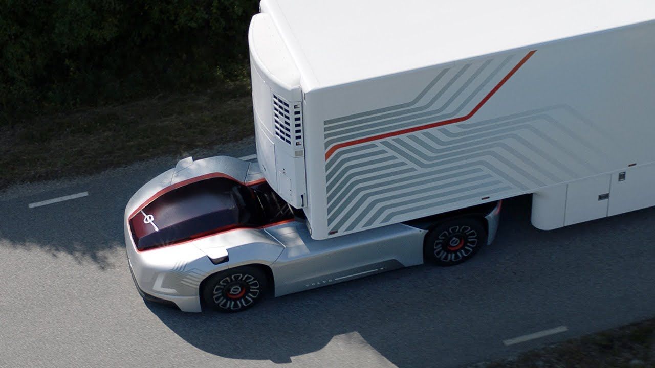
Vera, as the technology’s been dubbed, was unveiled in September, and consists of a sort of flat-Tesla-like electric car with a standard trailer hookup. The vehicles are connected to a cloud service, which also connects them to each other and to a control center. The control center monitors the trucks’ positioning (they’re designed to locate their position to within centimeters), battery charge, load content, service requirements, and other variables. The driveline and battery pack used in the cars are the same as those Volvo uses in its existing electric trucks.
You won’t see these cruising down an interstate highway, though, or even down a local highway. Vera trucks are designed to be used on short, repetitive routes contained within limited areas—think shipping ports, industrial parks, or logistics hubs. They’re limited to slower speeds than normal cars or trucks, and will be able to operate 24/7. “We will see much higher delivery precision, as well as improved flexibility and productivity,” said Mikael Karlsson, VP of Autonomous Solutions at Volvo Trucks. “Today’s operations are often designed according to standard daytime work hours, but a solution like Vera opens up the possibility of continuous round-the-clock operation and a more optimal flow. This in turn can minimize stock piles and increase overall productivity.”
Continue reading “No Safety Driver Here—Volvo’s New Driverless Truck Cuts the Cab” »


