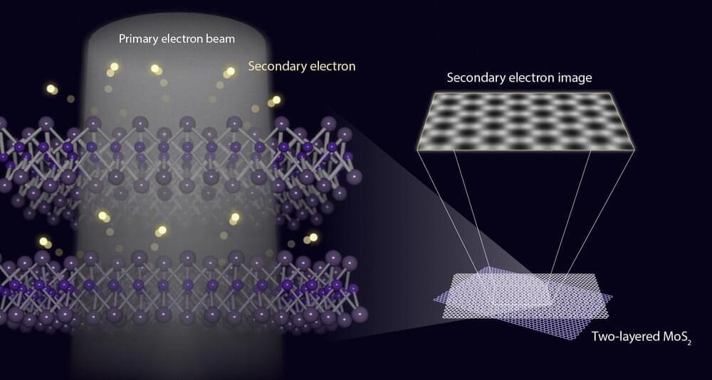
Surfaces play a key role in numerous chemical reactions, including catalysis and corrosion. Understanding the atomic structure of the surface of a functional material is essential for both engineers and chemists. Researchers at Nagoya University in Japan used atomic-resolution secondary electron (SE) imaging to capture the atomic structure of the very top layer of materials to better understand the differences from its lower layers. The researchers published their findings in the journal Microscopy.
Some materials exhibit “surface reconstruction,” where the surface atoms are organized differently from the interior atoms. To observe this, especially at the atomic level, surface-sensitive techniques are needed.
Traditionally, scanning electron microscopy (SEM) has been an effective tool to examine nanoscale structures. SEM works by scanning a sample with a focused electron beam and capturing the SEs emitted from the surface. SEs are typically emitted from a shallow depth below the surface, making it difficult to observe phenomena like surface reconstruction, especially if only a single atomic layer is involved.


