Menu

Blog

Archive for the ‘engineering’ category: Page 230

Oct 3, 2015

Polyera is a flexible electronics company

Posted by in categories: electronics, engineering

Founded in 2005, Polyera has developed deep and unique expertise spanning science, engineering, and design focused on flexible electronics.

Read more

Oct 3, 2015

Method to replace silicon with carbon nanotubes developed

Posted by in categories: computing, engineering, singularity

Moore’s Law is, and shall be for a very long time, the law of the land.
Singularity: +1, Luddites: Who cares, they don’t use computers.
wink


Schematic of a set of molybdenum (M0) end-contacted nanotube transistors (credit: Qing Cao et al./Science)

IBM Research has announced a “major engineering breakthrough” that could lead to carbon nanotubes replacing silicon transistors in future computing technologies.

Read more

Oct 2, 2015

Nanotube Electronics Could Replace Silicon — IBM Research Breakthrough

Posted by in categories: computing, electronics, engineering

IBM announced a major engineering breakthrough that could open the way to replacing silicon transistors with carbon nanotubes in future electronics and computing technologies.

Silicon transistors have become dramatically smaller in the last decades following Moore’s Law — the observation that the number of transistors per unit area doubles every two tears. However, silicon transistor technology is approaching a point of physical limitation.

With Moore’s Law running out of steam, shrinking the size of transistors — including the channels and contacts — without compromising performance is a research and manufacturing challenge. Carbon nanotube technology could lead to much smaller transistors and keep electronics and computing devices on the Moore’s Law of exponentially decreasing size and thus increasing performance. However, as devices become smaller, increased contact resistance for carbon nanotubes has hindered performance gains until now.

Read more

Oct 1, 2015

IBM unlocks the secret to carbon nanotube transistors

Posted by in categories: computing, engineering, internet, materials, neuroscience

Following Moore’s law is getting harder and harder, especially as existing components reach their physical size limitations. Parts like silicon transistor contacts — the “valves” within a transistor that allow electrons to flow — simply can’t be shrunken any further. However, IBM announced a major engineering achievement on Thursday that could revolutionize how computers operate: they’ve figured out how to swap out the silicon transistor contacts for smaller, more efficient, carbon nanotubes.

The problem engineers are facing is that the smaller silicon transistor contacts get, the higher their electrical resistance becomes. There comes a point where the components simply get too small to conduct electrons efficiently. Silicon has reached that point. But that’s where the carbon nanotubes come in. These structures measure less than 10 nanometers in diameter — that’s less than half the size of today’s smallest silicon transistor contact. IBM actually had to devise a new means of attaching these tiny components. Known as an “end-bonded contact scheme” the 10 nm electrical leads are chemically bonded to the metal substructure. Replacing these contacts with carbon nanotubes won’t just allow for computers to crunch more data, faster. This breakthrough ensures that they’ll continue to shrink, following Moore’s Law, for several iterations beyond what silicon components are capable of.

“These chip innovations are necessary to meet the emerging demands of cloud computing, Internet of Things and Big Data systems,” Dario Gil, vice president of Science & Technology at IBM Research, said in a statement. “As technology nears the physical limits of silicon, new materials and circuit architectures must be ready to deliver the advanced technologies that will drive the Cognitive Computing era. This breakthrough shows that computer chips made of carbon nanotubes will be able to power systems of the future sooner than the industry expected.” The study will be formally published October 2nd, in the journal Science. This breakthrough follows a number of other recent minimization milestones including transistors that are only 3-atoms thick or constructed from a single atom.

Read more

Sep 29, 2015

Terraforming Mars: Things to do to make Mars habitable

Posted by in categories: engineering, environmental, space

Terraforming can be approximately defined as transforming the state of any heavenly bodies such as moons, planets to that of Earth.

Read more

Sep 26, 2015

New system for human genome editing has potential to increase power and precision of DNA engineering

Posted by in categories: biotech/medical, engineering

CRISPR-Cpf1 offers simpler approach to editing DNA; technology could disrupt scientific and commercial landscape.

Read more

Sep 24, 2015

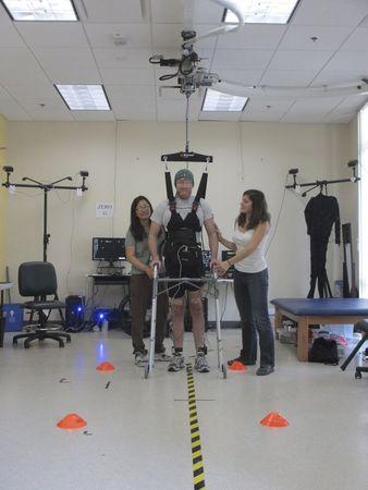
Brain-computer link enables paralyzed California man to walk

Posted by in categories: biotech/medical, computing, engineering, information science, neuroscience, robotics/AI

By Steve Gorman LOS ANGELES (Reuters) — A brain-to-computer technology that can translate thoughts into leg movements has enabled a man paralyzed from the waist down by a spinal cord injury to become the first such patient to walk without the use of robotics, doctors in Southern California reported on Wednesday. The slow, halting first steps of the 28-year-old paraplegic were documented in a preliminary study published in the British-based Journal of NeuroEngineering and Rehabilitation, along with a YouTube video. The feat was accomplished using a system allowing the brain to bypass the injured spinal cord and instead send messages through a computer algorithm to electrodes placed around the patient’s knees to trigger controlled leg muscle movements.

Read more

Sep 23, 2015

Engineering Humans for War

Posted by in categories: computing, cyborgs, electronics, engineering, military

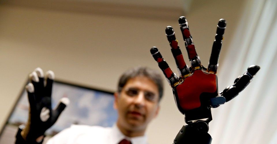
For decades after its inception in 1958, the Defense Advanced Research Projects Agency—DARPA, the central research and development organization of the Department of Defense—focused on developing vast weapons systems. Starting in 1990, and owing to individuals like Gorman, a new focus was put on soldiers, airmen, and sailors—on transforming humans for war. The progress of those efforts, to the extent it can be assessed through public information, hints at war’s future, and raises questions about whether military technology can be stopped, or should.

Gorman sketched out an early version of the thinking in a paper he wrote for DARPA after his retirement from the Army in 1985, in which he described an “integrated-powered exoskeleton” that could transform the weakling of the battlefield into a veritable super-soldier. The “SuperTroop” exoskeleton he proposed offered protection against chemical, biological, electromagnetic, and ballistic threats, including direct fire from a.50-caliber bullet. It “incorporated audio, visual, and haptic [touch] sensors,” Gorman explained, including thermal imaging for the eyes, sound suppression for the ears, and fiber optics from the head to the fingertips. Its interior would be climate-controlled, and each soldier would have his own physiological specifications embedded on a chip within his dog tags. “When a soldier donned his ST [SuperTroop] battledress,” Gorman wrote, “he would insert one dog-tag into a slot under the chest armor, thereby loading his personal program into the battle suit’s computer,” giving the 21st-century soldier an extraordinary ability to hear, see, move, shoot, and communicate.

Read more

Sep 22, 2015

Digestible batteries needed to power electronic pills

Posted by in categories: biotech/medical, electronics, engineering, materials

Imagine a “smart pill” that can sense problems in your intestines and actively release the appropriate drugs. We have the biological understanding to create such a device, but we’re still searching for electronic materials (like batteries and circuits) that pose no risk if they get stuck in our bodies. In Trends in Biotechnology on September 21, Christopher Bettinger of Carnegie Mellon University presents a vision for creating safe, consumable electronics, such as those powered by the charged ions within our digestive tracts.

Edible electronic medical devices are not a new idea. Since the 1970s, researchers have been asking people to swallow prototypes that measure temperature and other biomarkers. Currently, there are ingestible cameras for gastrointestinal surgeries as well as sensors attached to medications used to study how drugs are broken down in the body.

“The primary risk is the intrinsic toxicity of these materials, for example, if the battery gets mechanically lodged in the gastrointestinal tract–but that’s a known risk. In fact, there is very little unknown risk in these kinds of devices,” says Bettinger, a professor in materials science and engineering. “The breakfast you ate this morning is only in your GI tract for about 20 hours–all you need is a battery that can do its job for 20 hours and then, if anything happens, it can just degrade away.”

Read more

Sep 21, 2015

Crystallizing the DNA nanotechnology dream: Scientists have designed the first large DNA crystals

Posted by in categories: biotech/medical, chemistry, computing, engineering, materials, nanotechnology

DNA has garnered attention for its potential as a programmable material platform that could spawn entire new and revolutionary nanodevices in computer science, microscopy, biology, and more. Researchers have been working to master the ability to coax DNA molecules to self assemble into the precise shapes and sizes needed in order to fully realize these nanotechnology dreams.

For the last 20 years, scientists have tried to design large DNA crystals with precisely prescribed depth and complex features – a design quest just fulfilled by a team at Harvard’s Wyss Institute for Biologically Inspired Engineering. The team built 32 DNA crystals with precisely-defined depth and an assortment of sophisticated three-dimensional (3D) features, an advance reported in Nature Chemistry.

The team used their “DNA-brick self-assembly” method, which was first unveiled in a 2012 Science publication when they created more than 100 3D complex nanostructures about the size of viruses. The newly-achieved periodic crystal structures are more than 1000 times larger than those discrete DNA brick structures, sizing up closer to a speck of dust, which is actually quite large in the world of DNA nanotechnology.

Read more