Archive for the ‘materials’ category: Page 15
Sep 20, 2024
Potential and challenges of computing with molecular materials
Posted by Dan Breeden in categories: computing, materials
Molecular materials for computing progress intensively but the performance and reliability still lag behind. Here the authors assess the current state of computing with molecular-based materials and describe two issues as the basis of a new computing technology: continued exploration of molecular electronic properties and process development for on-chip integration.
Sep 20, 2024
New Device Leads to “Dendrocentric Learning”
Posted by Dan Breeden in categories: materials, neuroscience
Sep 18, 2024
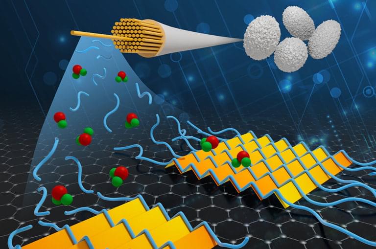
2D silk protein layers on graphene pave the way for advanced microelectronics and computing
Posted by Genevieve Klien in categories: computing, materials
After thousands of years as a highly valuable commodity, silk continues to surprise. Now it may help usher in a whole new direction for microelectronics and computing.
Sep 18, 2024
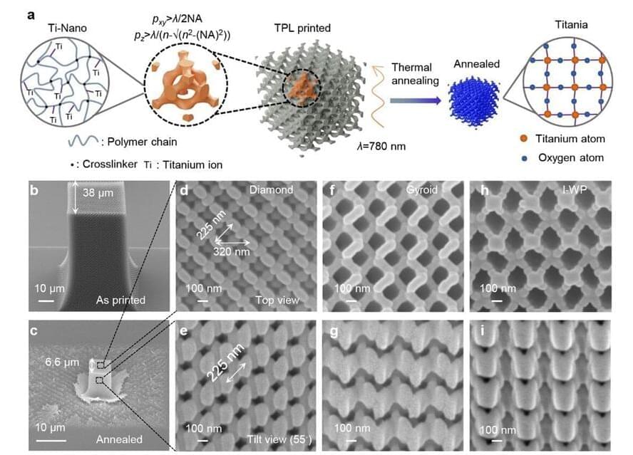
An unprecedented feat: Printing 3D photonic crystals that completely block light
Posted by Dan Breeden in category: materials
Photonic crystals are materials with repeating internal structures that interact with light in unique ways. We can find natural examples in opals and the vibrant colored shells of some insects. Even though these crystals are made of transparent materials, they exhibit a “photonic bandgap” that blocks light at certain wavelengths and directions.
Sep 18, 2024
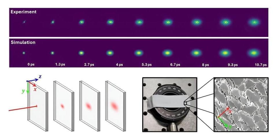
New method improves understanding of light-wave propagation in anisotropic materials
Posted by Saúl Morales Rodriguéz in categories: biotech/medical, materials
Understanding how light travels through various materials is essential for many fields, from medical imaging to manufacturing. However, due to their structure, materials often show directional differences in how they scatter light, known as anisotropy. This complexity has traditionally made it difficult to accurately measure and model their optical properties. Recently, researchers have developed a new technique that could transform how we study these materials.
Sep 18, 2024
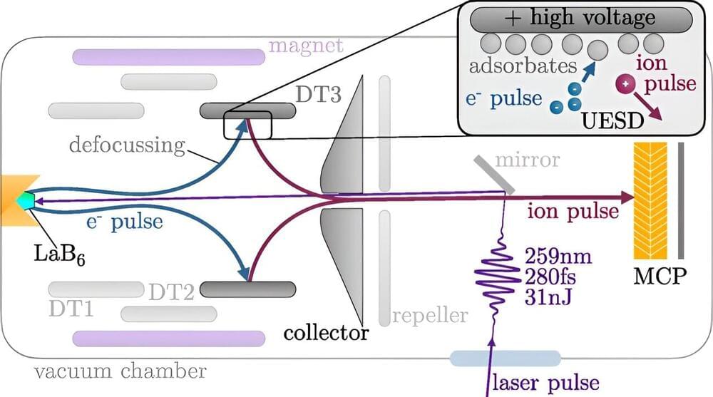
New technology produces ultrashort ion pulses
Posted by Saúl Morales Rodriguéz in categories: chemistry, materials
TU Wien (Vienna) has succeeded in generating laser-synchronized ion pulses with a duration of well under 500 picoseconds, which can be used to observe chemical processes on material surfaces. The work has been published in Physical Review Research.
Sep 17, 2024
Human bone-inspired cement is 5 times tougher than standard concrete
Posted by Raphael Ramos in categories: biotech/medical, materials
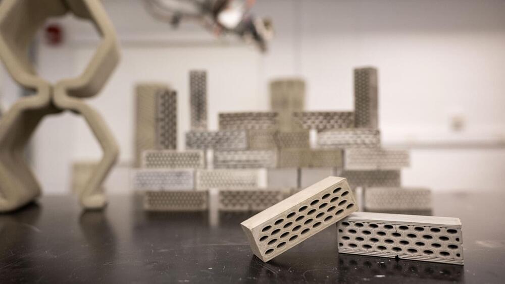
Getting tips from the design of the human body.
Scientists create bone-inspired cement, over five times stronger than concrete.
Continue reading “Human bone-inspired cement is 5 times tougher than standard concrete” »
Sep 16, 2024
Research team uses terahertz pulses of light to shed light on superconducting disorder
Posted by Saúl Morales Rodriguéz in category: materials
A team of researchers from the Max Planck Institute for the Structure and Dynamics of Matter (MPSD) in Hamburg, Germany, and Brookhaven National Laboratory in the United States has demonstrated a new way to study disorder in superconductors using terahertz pulses of light.
Sep 16, 2024
Smart graphene sensor sniffs out ammonia to keep beef fresh
Posted by Dan Breeden in categories: food, materials
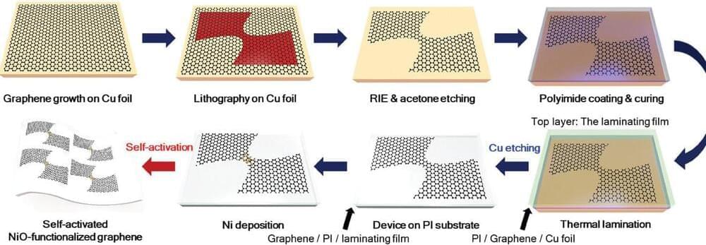
NiO-functionalized graphene sensor detects ammonia in real time, offering a powerful tool for monitoring beef freshness and ensuring food safety.


