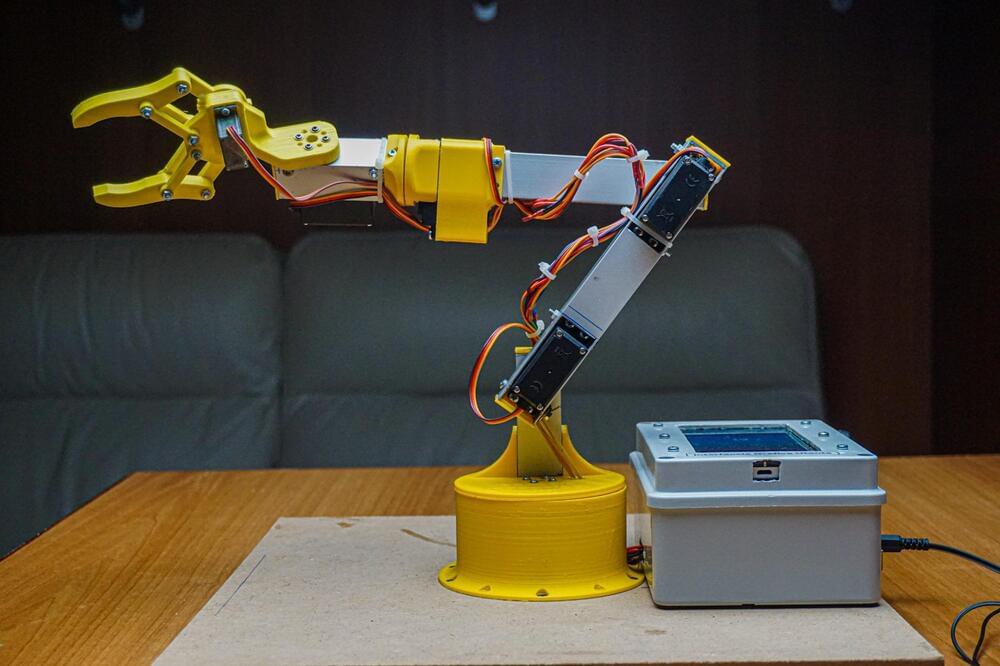
Normally, robotic arms are controlled by a GUI running on a host PC, or with some kind of analog system that maps human inputs to various degrees of rotation. However, Maurizio Miscio was able to build a custom robotic arm that is completely self-contained — thanks to a companion mobile app that resides on an old smartphone housed inside a control box.
Miscio started his project by making 3D models of each piece, most of which were 3D-printed. These included the gripper, various joints that each give a single axis of rotation, and a large circular base that acts as a stable platform on which the arm can spin. He then set to work attaching five servo motors onto each rotational axis, along with a single SG90 micro servo motor for the gripper. These motors were connected to an Arduino Uno that also had an HC-05 Bluetooth® serial module for external communication.
In order to operate the arm, Miscio developed a mobile app with the help of MIT App Inventor, which presents the user with a series of buttons that rotate a particular servo motor to the desired degree. The app even lets a series of motion be recorded and “played back” to the Uno over Bluetooth for repeated, accurate movements.



 עברית (Hebrew)


