Menu

Blog

Archive for the ‘materials’ category: Page 125

Nov 9, 2022

Atomic changes in metals could lead to longer-lasting batteries

Posted by in categories: materials, transportation

Researchers at Pacific Northwest National Laboratory (PNNL) are studying the atomic-level changes in metals undergoing shear deformation in order to deduce the effects of physical forces on these materials, according to a report by Phys.org published on Monday.

The work could lead to many new and improved applications such as longer-lasting batteries and lighter vehicles.

Nov 9, 2022

Magnetism or no magnetism? The influence of substrates on electronic interactions

Posted by in categories: energy, materials

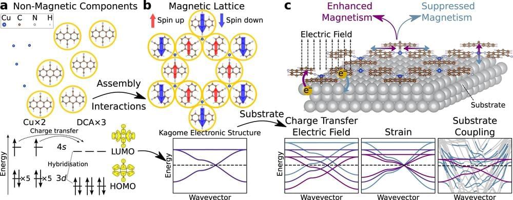
A new study at Monash University illustrates how substrates affect strong electronic interactions in two-dimensional metal-organic frameworks.

Materials with strong electronic interactions can have applications in energy-efficient electronics. When these materials are placed on a , their are changed by charge transfer, strain, and hybridization.

The study also shows that electric fields and applied strain could be used to “switch” interacting phases such as on and off, allowing potential applications in future energy-efficient electronics.

Nov 9, 2022

Materials Made of Mechanical Neural Networks Can Learn to Adapt Their Physical Properties

Posted by in categories: materials, robotics/AI

A new type of material can learn and improve its ability to deal with unexpected forces thanks to a unique lattice structure with connections of variable stiffness, as described in a new paper by my colleagues and me.

The new material is a type of architected material, which gets its properties mainly from the geometry and specific traits of its design rather than what it is made out of. Take hook-and-loop fabric closures like Velcro, for example. It doesn’t matter whether it is made from cotton, plastic or any other substance. As long as one side is a fabric with stiff hooks and the other side has fluffy loops, the material will have the sticky properties of Velcro.

My colleagues and I based our new material’s architecture on that of an artificial neural network—layers of interconnected nodes that can learn to do tasks by changing how much importance, or weight, they place on each connection. We hypothesized that a mechanical lattice with physical nodes could be trained to take on certain mechanical properties by adjusting each connection’s rigidity.

Nov 7, 2022

Gate-tunable heterojunction tunnel triodes based on 2D metal selenide and 3D silicon

Posted by in categories: computing, materials

Electronics engineers worldwide are trying to improve the performance of devices, while also lowering their power consumption. Tunnel field-effect transistors (TFETs), an experimental class of transistors with a unique switching mechanism, could be a particularly promising solution for developing low-power electronics.

Despite their potential, most TFETs based on silicon and III-V heterojunctions exhibit low on-current densities and on/off current ratios in some modes of operation. Fabricating these transistors using 2D materials could help to improve electrostatic control, potentially increasing their on-current densities and on/off ratios.

Researchers at University of Pennsylvania, the Chinese Academy of Sciences, the National Institute of Standards and Technology, and the Air Force Research Laboratory have recently developed new heterojunction tunnel triodes based on van der Waals heterostructures formed from 2D metal selenide and 3D silicon. These triodes, presented in a paper published in Nature Electronics, could outperform other TFETs presented in the past in terms of on-current densities and on/off ratios.

Nov 7, 2022

Artificial intelligence deciphers detector ‘clouds’ to accelerate materials research

Posted by in categories: materials, robotics/AI

X-rays can be used like a superfast, atomic-resolution camera, and if researchers shoot a pair of X-ray pulses just moments apart, they get atomic-resolution snapshots of a system at two points in time. Comparing these snapshots shows how a material fluctuates within a tiny fraction of a second, which could help scientists design future generations of super-fast computers, communications, and other technologies.

Resolving the information in these X-ray snapshots, however, is difficult and time intensive, so Joshua Turner, a lead scientist at the Department of Energy’s SLAC National Accelerator Center and Stanford University, and ten other researchers turned to artificial intelligence to automate the process. Their machine learning-aided method, published October 17 in Structural Dynamics, accelerates this X-ray probing technique, and extends it to previously inaccessible materials.

“The most exciting thing to me is that we can now access a different range of measurements, which we couldn’t before,” Turner said.

Nov 7, 2022

New camera system taps into terahertz wavelengths for better imaging

Posted by in categories: materials, security

A team of engineers has developed a new type of camera that can detect radiation in terahertz (THz) wavelengths. This new imaging system can see through certain materials in high detail, which could make it useful for security scanners and other sensors.

Terahertz radiation is that which has wavelengths between microwaves and visible light, and these frequencies show promise in a new class of imaging systems. They can penetrate many materials and capture new levels of detail, and importantly the radiation is non-ionizing, meaning it’s safer than X-rays when used on humans.

The problem is that detectors that pick up THz wavelengths can be bulky, slow, expensive, difficult to run under practical conditions, or some combination of these. But in a new study, researchers at MIT, Samsung and the University of Minnesota have developed a system that can detect THz pulses quickly, precisely and at regular room temperature and pressure.

Nov 6, 2022

TSMC approaching 1 nm with 2D materials breakthrough

Posted by in categories: computing, materials

TSMC is setting up a new 1-nm chip production facility that will be located in an industrial park in Longtan District in Taiwan.

Nov 5, 2022

Is This the Best Semiconductor Ever Found?

Posted by in category: materials

Scientists have discovered that an obscure material known as cubic boron arsenide (c-BAs) may perform much better than silicon. In fact, it may be the best semiconductor possible—demonstrating both high carrier mobility and simultaneously high thermal conductivity.

Nov 3, 2022

Graphene Membrane Forms a Soft, Stretchable Wearable Heater

Posted by in categories: materials, wearables

Wearable heaters are highly desirable for low-temperature environments. However, the fundamental challenge in achieving such devices is to design electric-heating membranes with flexible, breathable, and stretchable properties.

Study: Large-Scale Preparation of Micro–Nanofibrous and Fluffy Propylene-Based Elastomer/ [email protected] Nanoplatelet Membranes with Breathable and Flexible Characteristics for Wearable Stretchy Heaters. Image Credit: s_maria/Shutterstock.com.

A study published in ACS Applied Materials and Interfaces aimed to achieve an electric heating membrane with a nanofibrous fluffy texture and excellent electric-heating features. Here, an electric heating membrane was fabricated by coating a melt-blown propylene-based elastomer (PBE) with polyurethane (PU) and graphene nanoplatelet films via an easy, cost-effective, and large-scale method involving a coating-compression cyclic process.

Nov 3, 2022

Machine-Learning Tool Solves Metamaterial Jigsaw

Posted by in categories: materials, robotics/AI

A new tool can determine whether a collection of building blocks will assemble into a mechanically sound structure.